Semiconductor Equipment Parts CNC Machining
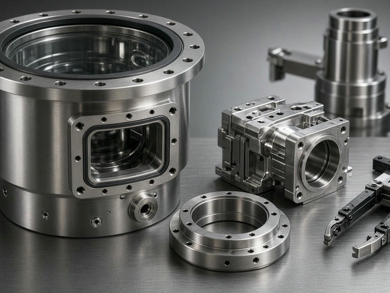
Engineered components meeting stringent geometric tolerances, critical vacuum integrity, and tight positional relationships. We manufacture custom vacuum chambers, wafer handling parts, and precision structural housings for global equipment OEMs.
Engineering Challenges in Semiconductor Component Manufacturing
Manufacturing for semiconductor precision parts and vacuum equipment machining extends far beyond routine milling. We address the thermal, mechanical, and surface constraints critical to high-performance fab environments.
Deep-Cavity & Thin-Wall Milling
Complex vacuum chambers require aggressive material removal while preventing structural warping. Optimized toolpaths and balanced roughing-to-finishing cycles preserve dimensional stability across thin-wall structures.
High-Density Hole Patterns
Multi-port vacuum equipment housings require exact true-position tolerances across hundreds of threaded and through-hole locations to ensure dependable O-ring sealing and vacuum seal integrity.
Multi-Setup Error Elimination
By shifting complex geometries to simultaneous 5-axis machining platforms, we eliminate cumulative repositioning errors and maintain strict perpendicularity and flatness between interfacing planes.
Precision Machining Capabilities & Equipment Inventory
Our facility is configured for tight-tolerance semiconductor and automation assemblies, anchored by synchronized Japanese machining centers with 0.003 mm machine positioning precision.
| Equipment Model | Machining Envelope / Capacity | Core Specifications | Quantity |
|---|---|---|---|
| Mazak C600 5-Axis | 900 × 900 × 700 mm | 24,000 rpm high-speed spindle | 8 units |
| Mazak VCN-430AL 4-Axis | 560 × 430 × 510 mm | 12,000 rpm spindle | 39 units |
| Mazak HCN5000 Horizontal | 560 × 430 × 510 mm | 12,000 rpm spindle | 2 units |
| Mazak QTC100MY Turn-Mill | Φ350 / 500 mm | 6,000 rpm spindle | 10 units |
Material Systems & Application Mapping
Aluminum (6061, 7075)
Primary choice for lightweight structural frames, end effectors, and vacuum load locks requiring strict dimensional stability.
Structural & EnclosuresStainless (303, 304, 316L)
High vacuum chambers, gas delivery blocks, and chemical handling assemblies demanding oxidation resistance and vacuum seal longevity.
Vacuum & FluidicsCopper & Copper Alloys
RF showerheads, heat sink pedestals, and thermal management units requiring high electrical and thermal conductivity.
Thermal ManagementEngineering Plastics (PEEK, PPS)
Wafer-contact guides, chemical-resistant CMP parts, and dielectric isolators operating in harsh chemical bath environments.
Wafer Handling & InsulationInspection-Driven Manufacturing & Quality Verification
Semiconductor components must satisfy drawing limits for geometric dimensioning, vacuum seal smoothness, and material purity. Cleanliness, leak-tightness, and particulate criteria are verified strictly in adherence with customer-supplied specifications.
Full traceability and operational compliance under ISO 9001, AS9100D, and ISO 13485 standards.
ZEISS CMM
Envelope: 700 × 700 × 600 mm
Verifies 3D geometric true positions, co-axiality, and flatness on multi-port chambers and critical reference datum planes.
XRF DX-320L (1 Unit)
Spectrometric Verification
Provides raw-material elemental analysis and alloy authentication before cutting to prevent non-conforming lot contamination.
TR200 Roughness Meters (2 Units)
Ra / Rz Verification
Measures contact faces and dynamic sealing lands to ensure compliance with customer vacuum leak and sealing standards.
2.5D & Hardness Testers
Concentricity & Hardness
Includes non-contact optical measurement, concentricity checking benches, and Rockwell/Vickers hardness testers.
Supporting Your Equipment Lifecycle: EVT to Volume OEM
Whether validating an early proof-of-concept design or ramping batch production for commercial wafer fabs, we integrate engineering feedback early to optimize cycle times and cut scrap rates.
DFM Optimization
Comprehensive review of internal tool radii, draft angles, through-hole depths, and datum architectures before spindle startup to prevent machining bottlenecks.
Prototype & EVT/DVT
Rapid fabrication of engineering test samples with complete dimensional inspection records to validate functional vacuum and motion fitment.
Serial OEM Production
Scalable multi-axis machining capacity backed by strict revision control, traceability, and secure handling of sensitive CAD designs under NDA.
Frequently Asked Technical Questions
Common questions regarding semiconductor equipment part machining, materials, and tolerances.
Send Your Semiconductor Equipment Part Drawing
Upload your 2D/3D part drawings (.STEP, .IGES, .DWG) along with tolerance and surface finish requirements. Our engineering team will review your specifications, perform a DFM evaluation, and provide an itemized quote.